Korea’s Largest Semiconductor Substrate Company
Package substrates are used for core semiconductors in mobile devices and PCs, transmitting electrical signals between the semiconductor and the main board and protecting costly semiconductors from external stress. It is a high-density circuit board containing more microcircuits than general substrates, which can reduce assembly defects and costs associated with attaching expensive semiconductors directly to the main board.
Solutions
-
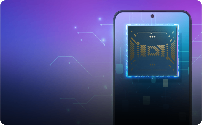
- FCCSP
- It is connected to the substrate in an inverted position via bumps rather than via wire bonding to the semiconductor, and is primarily used for high-performance semiconductors, such as APs (Application Processors) in mobile IT devices.
-
- WBCSP
- A product in which the semiconductor chip and package substrate are connected by gold wire, and the semiconductor chip size is greater than 80% of the substrate area.
-
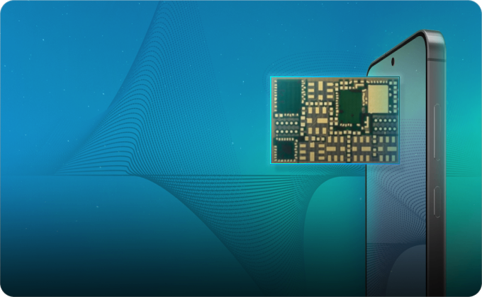
- SiP
- A product that realizes complex functions as one system by mounting multiple ICs and passive components in a package and has heat dissipation characteristics.
-

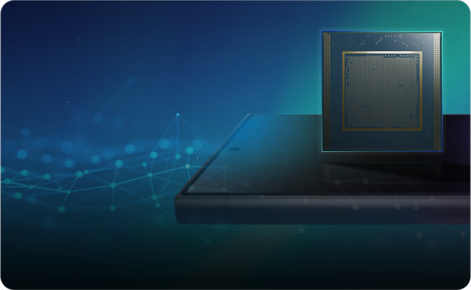
- FCBGA
- A high-density package substrate for connecting a high-integration semiconductor chip to a main board. The semiconductor chip and the package substrate are connected with Flip Chip bumps.
Curation
Sign up for our newsletter to receive news and valuable information about Samsung Electro-Mechanics.
SubscribeFAQ
-
The BGA production base is the domestic Sejong Plant, and the FCBGA products are produced at the domestic Busan Plant and the overseas Vietnamese production base.
-
FCBGA is used in a variety of fields from PC and game device to Data Center and automobiles, etc.
- Client: CPU and GPU for Desktop and Note PC, SoC for Game Console
- HPC: CPU for Server, ASIC for AI accelerator
- Network: ASIC for Router/Switch
- Automotive: SoC for ADAS, Radar and Infotainment
-
When you go to the Contact us on the main page or the Product page, you can ask questions about technologies and purchases by each region.
-
Samsung Electro-Mechanics mainly provides OSP and ENEPIG methods for FCBGA surface processing but can also develop and respond to new surface processing methods if necessary.
-
For BGA products, we mainly provide methods such as ENEPIG, Ni/Au, and Direct Au, and electrolytic Ni/Au can be categorized into thick Ni/Au and thin Ni/Au.